|
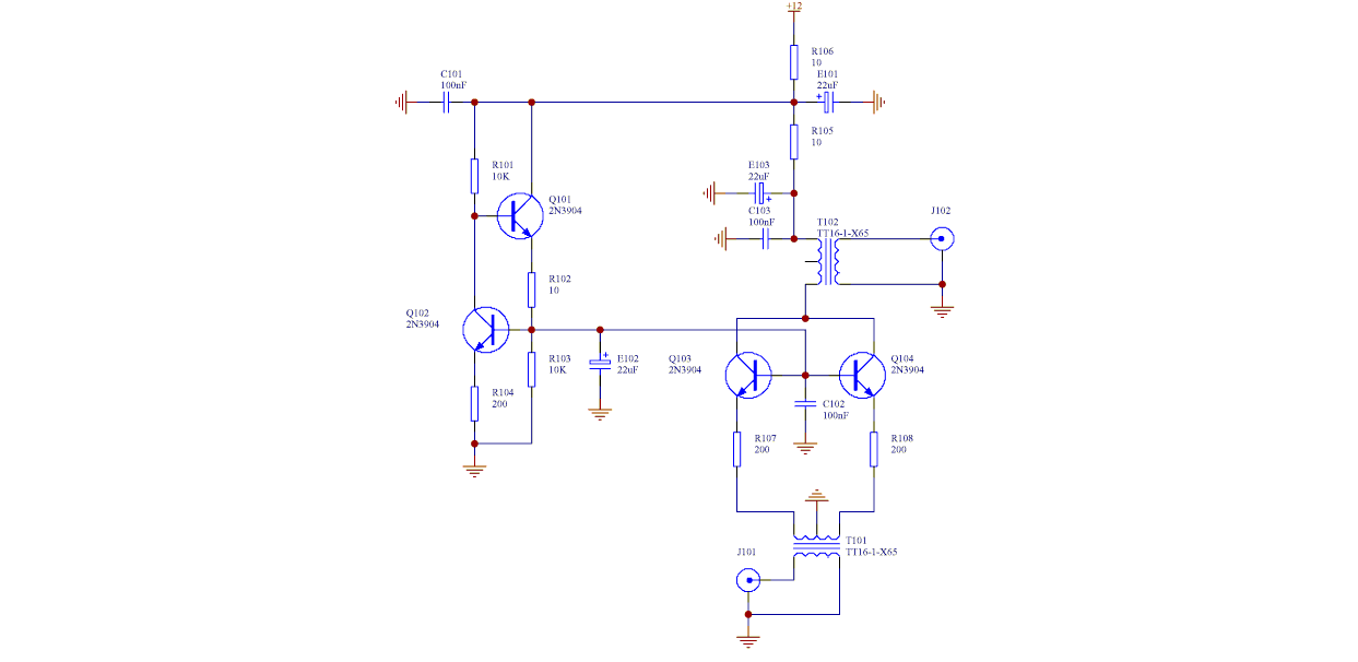
The low phase noise common base BJT frequency doubler shown above is capable of very good performance despite the fact that it uses inexpensive transistors. The low dc gain from base to collector of the dual transistor coupled with the emitter degeneration ensures low phase noise performance. The circuit is intended for use with 5MHz or 10MHz input frequencies.
Like all frequency doublers it has lowest output phase noise with higher input signals. it is designed for an input of +13dBm and is intended to drive a 50 ohm load (higher load impedances may cause the transistors to enter saturation). The combined collector waveform is a rectified sinewave superimposed on a small dc offset.Lowest signal phase instability is obtained when a low pass filter with low phase shift at the desired output frequency(2f) is combined with relatively high Q series tuned circuits connected between the common collectors and ground. These tuned circuits suppress the unwanted frequency components in the output (fundamental (f) 3f, 4f etc). The components at f, 3f, 5f etc are due to inevitable trasistor and transformer mismatches, however they will have realtively low amplitudes. The high Q series resonant (at f, 3f, 5f etc) tuned circuits will contribute little phase shift and associated instability at the desired 2f output frequency.
TBD..
http://tf.nist.gov/timefreq/general/pdf/498.pdf
http://tf.nist.gov/timefreq/general/pdf/1134.pdf
http://tf.nist.gov/timefreq/general/pdf/1139.pdf
http://tf.nist.gov/timefreq/general/pdf/1200.pdf
http://tf.nist.gov/timefreq/general/pdf/1244.pdf
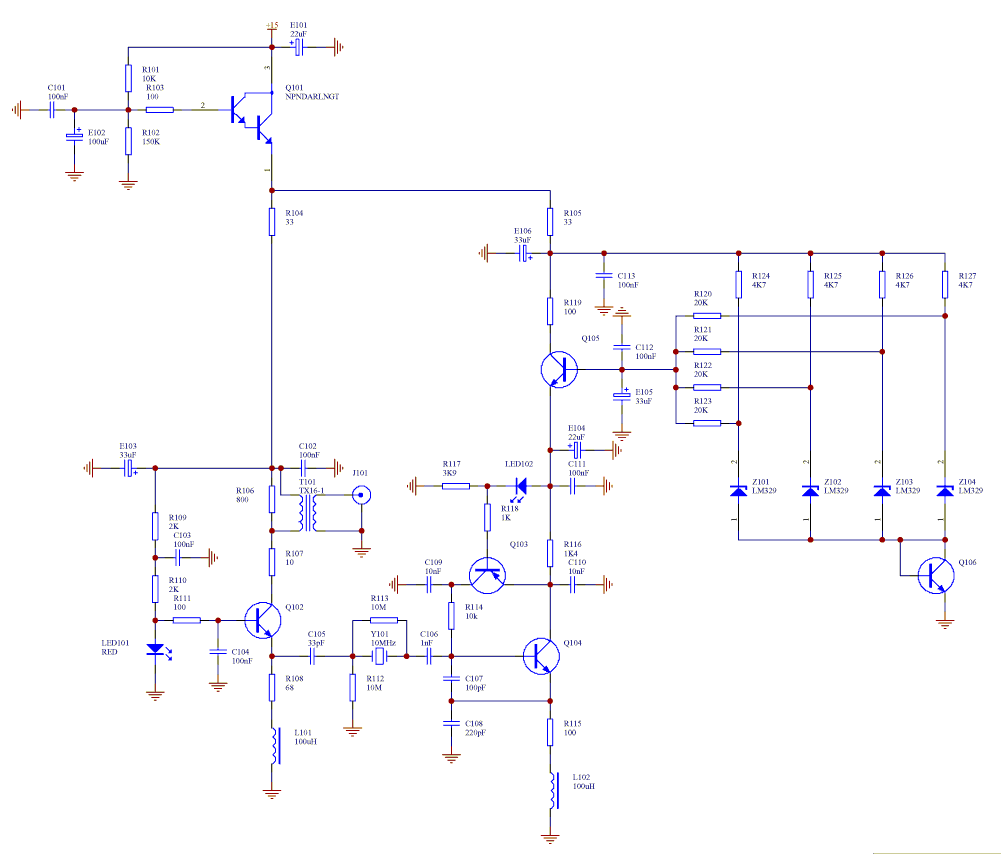 |
The above circuit illustrates several low noise techiques as applied to a low noise crystal oscillator.
The circuit is only suitable for fundamental crystals as there are no mode suppression components. The oscillator transistor Q104 is cutoff most of the time except for a short period at the peak of the crystal curent waveform. Q103 regulates the dc collector current of the oscillator transistor Q103. The dc collector current of Q104 and hence the crystal current is set by the value of R116.
Darlington transistor Q101 buffers the output of the filter (R101, R102, C101, E102) which low pass filters the power supply noise above 0.16Hz. The oscillator supply voltage is produced by low pass filtering the average output of 4x LM329 buried zener references (Z101-Z103). Q105 buffers the low pass filter output and Q106 compensates for the base emitter voltage drop of Q105.
The collector base voltage of the oscillator transistor Q104 is relatively high to reduce its collector base capacitance and its voltage sensitivity. This, together with the low dc gain from Q104 base to collector, keeps Q104's contribution to the oscillator flicker phase noise low. Common base buffer transistor Q102 has a low dc gain (0.5x) from base to collector, its emitter current is set by LED101, and R108 so that the buffer flicker phase noise is low.
The low noise oscillator power supply ensures that the modulation of oscillator transistor collector base capacitance by power supply noise and hence the power supply induced oscillator phase noise is low.
For further examples see:
additional Crystal Oscillators
TBC..