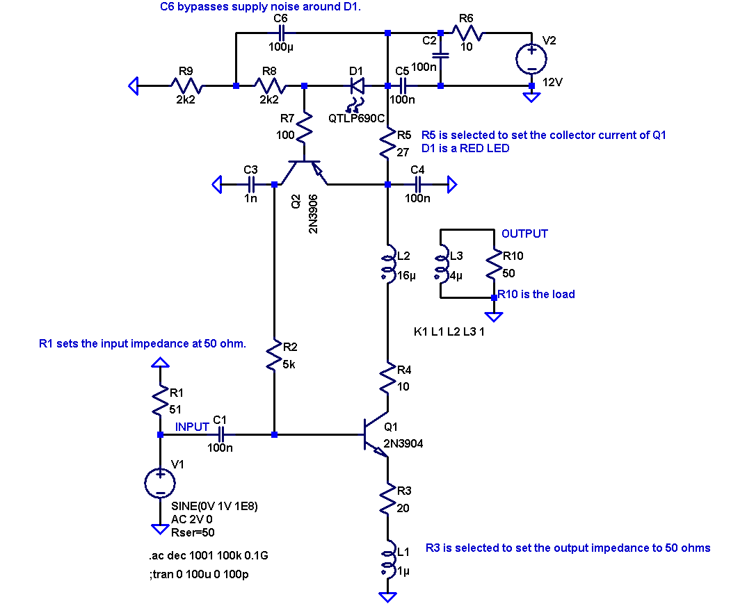
The well known Norton transformer feedback amplifier uses a common base amplifier with transformer feedback from the collector to the emitter. The transformer turns ratios are selected to set the gain and match the output to the load. The resultant amplifier has very low phase noise but low reverse isolation. For use as a buffer for a frequency source an amplifier with somewhat higher reverse isolation is desirable. Conventional common base amplifiers with series resistive feedback have significantly higher reverse isolation but suffer from input distortion and, if high impedance collector loads are used, output distortion due to output capacitance nonlinearity becomes apparent.One solution is to use a common emitter amplifier with series transformer feedback in the emitter circuit. However a resistor in series with the emitter is then required to match the output impedance to the load. The resultant amplifier has a reverse isolation comparable to that of a series resistive feedback common base stage with lower nonlinearity and noise. The reverse isolation for a low gain amplifier is largely determined by the hfe of the transistor at the operating frequency so the ft of the transistor should be significantly higher than the input frequency to avoid degrading the reverse isolation. Typically a reverse isolation of 40dB or so is readily achieved. A typical amplifier of this type is depicted below.
|
In this example the dc collector current of the RF transistor is stabilised by the pnp transistor which senses the voltage drop across R and compares it with the ~1V reference formed by the difference between the LED forward voltage drop and the Vbe of pnp transistor. The RF gain is largely determined by the transformer output to emitter turns ratio (voltage gain ~ n/2) whilst the resistor in series with the emitter is selected to set the output impedance. The amplifier works best when the gain is small (<10dB or so). For isolation amplifier applications one can cascade several such low gain amplifiers to achieve the required reverse isolation as long as sufficient care is taken to minimise coupling via the power supply. With a suitable RF transistor output levels of +27dBm or more can be achieved if the dc collector current is high enough. Since some of the output current us supplied by the emitter circuit and the feedback is effective in reducing distortion the dc collector current can actually be a little smaller than the peak RF load current without significantly increasing the distortion.
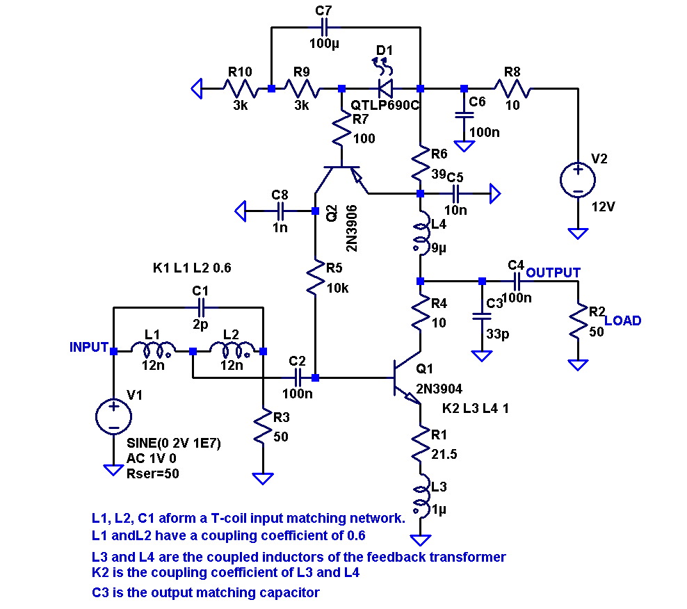
The input impedance can be set to 50 ohms by shunting the input with a low value (~50 ohm) resistor. A better input match is achieved at high frequencies if a bridged T-coil circuit is used between the source, the RF transistor base and the input terminating resistor. This also has the effect of increasing the circuit bandwidth, however it doesnt improve the high frequency reverse isolation. The high frequency output match can be improved by shunting the output with a capacitor. In the circuit shown below a bridged T-coil network is used to improve the input match whilst a shunt capacitor improves the output match.
 |
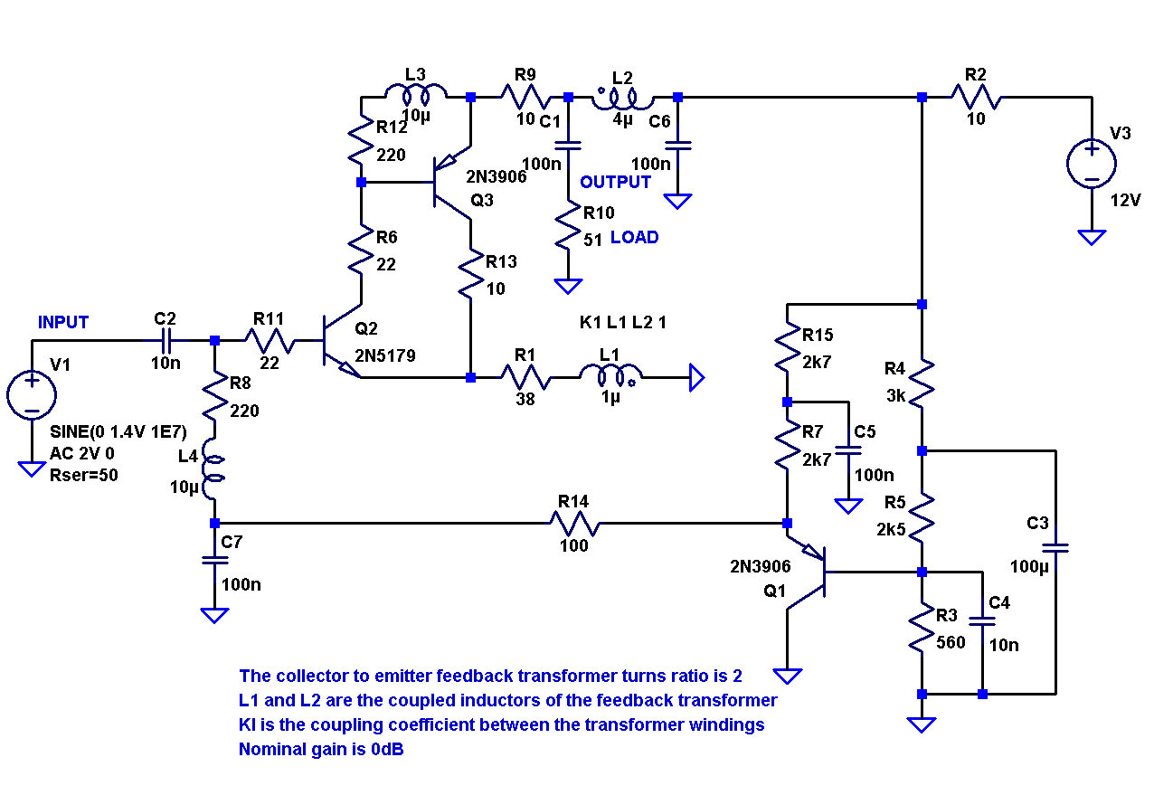
If one substitutes a Sziklai pair for the RF transistor the distortion performance can be significantly improved along with the reverse isolation. However in order to ensure that the Sziklai pair doesnt oscillate the input device should have a significantly higher ft that the output device. Since the input transistor of the Sziklai pair has a relatively low dc base current a simpler biasing scheme like that depicted in the example shown below can be used. Simulation indicates that at the output IP2 ~ +80dBm and IP3 ~ +50dBm may be possible for the circuit shown.
 |
TBC...