When using an opamp as a low noise isolation amplifier, minimise the dc and low frequency noise gain of the opamp as this minimises the flicker phase modulation of the amplifier output. Power supply noise also modulates the opamp internal junction capacitances, etc., so a low noise power supply is essential for low flicker phase noise operation. Since the Johnson noise of feedback and input resistors in the circuit adds to the phase noise floor, keeping the vale of these resistors low minimises their contribution to the phase noise floor. Where cermet resistors (e.g. pots) are used then it is essential to minmise the dc current flowing in these components otherwise they generate considerable excess noise at low frequencies. Plastic, thick film and carbon resistors also generate excess noise when dc current flows in them, for lowest noise metal film resistors should be used. Opamps should be selected for low noise, particularly in the flicker region as well as adequate power bandwidth. In general current feedback opamps are unsuitable (at least for low gain stages) as the noise voltage developed by by the inverting input noise current flowing in the feedback resistor can be fairly large, particularly at low frequencies.
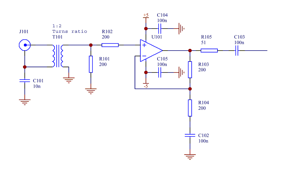
The circuit below illustrates a dual supply RF amplifier using a fixed gain opamp . The input transformer steps up the signal by 6dB to minimise the RF gain required. A noninverting amplifier is used as it has the lowest equivalent input noise for low RF gains. C102 ensures that the opamp dc gain and low frequency gain is low minimising the low frequency noise voltages across internal junctions and hence the opamp self noise flicker phase modulation. The feedback network and input protection resistors values are low to keep their contribution to the noise floor well below that of the opamp. C102 also ensures that the dc current flowing in the feedback resistor network is very low.
|
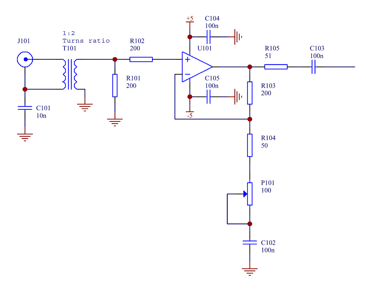
The circuit below illustrates a dual supply variable gain RF amplifier using an opamp. The input transformer steps up the signal by 6dB to minimise the RF gain required. A noninverting amplifier is used as it has the lowest equivalent noise for low RF gains. C102 ensures that the opamp dc gain and low frequency gain is low minimising the low frequency noise voltages across internal junctions and hence the opamp self noise flicker phase modulation. The feedback network and input protection resistors values are low to keep their contribution to the noise floor well below that of the opamp. C102 also ensures that the dc current flowing in the feedback resistor network is very low so that a cermet pot can be used in the feedback network without adding significant excess noise.
 |
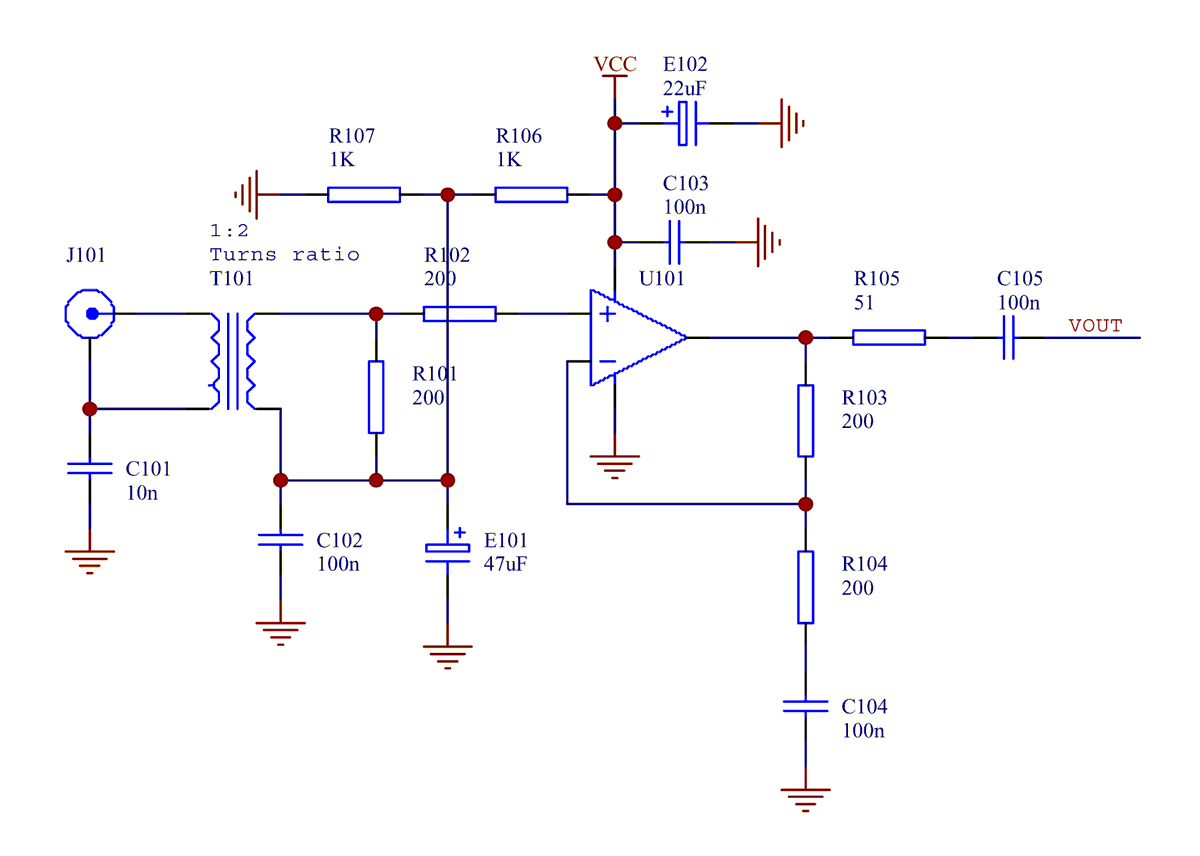
The circuit below illustrates a single supply fixed gain RF amplifier using an opamp. The input transformer steps up the signal by 6dB to minimise the RF gain required. A noninverting amplifier is used as it has the lowest equivalent noise for low RF gains. C104 ensures that the opamp dc gain and low frequency gain is low minimising the low frequency noise voltages across internal junctions and hence the opamp self noise flicker phase modulation. The feedback network and input protection resistors values are low to keep their contribution to the noise floor well below that of the opamp. C104 also ensures that the dc current flowing in the feedback resistor network is very low. R101, R102, E101, C102 are used to generate a low noise voltage divider to bias the transformer secondary and opamp noninverting input at 1/2 the supply voltage.
 |
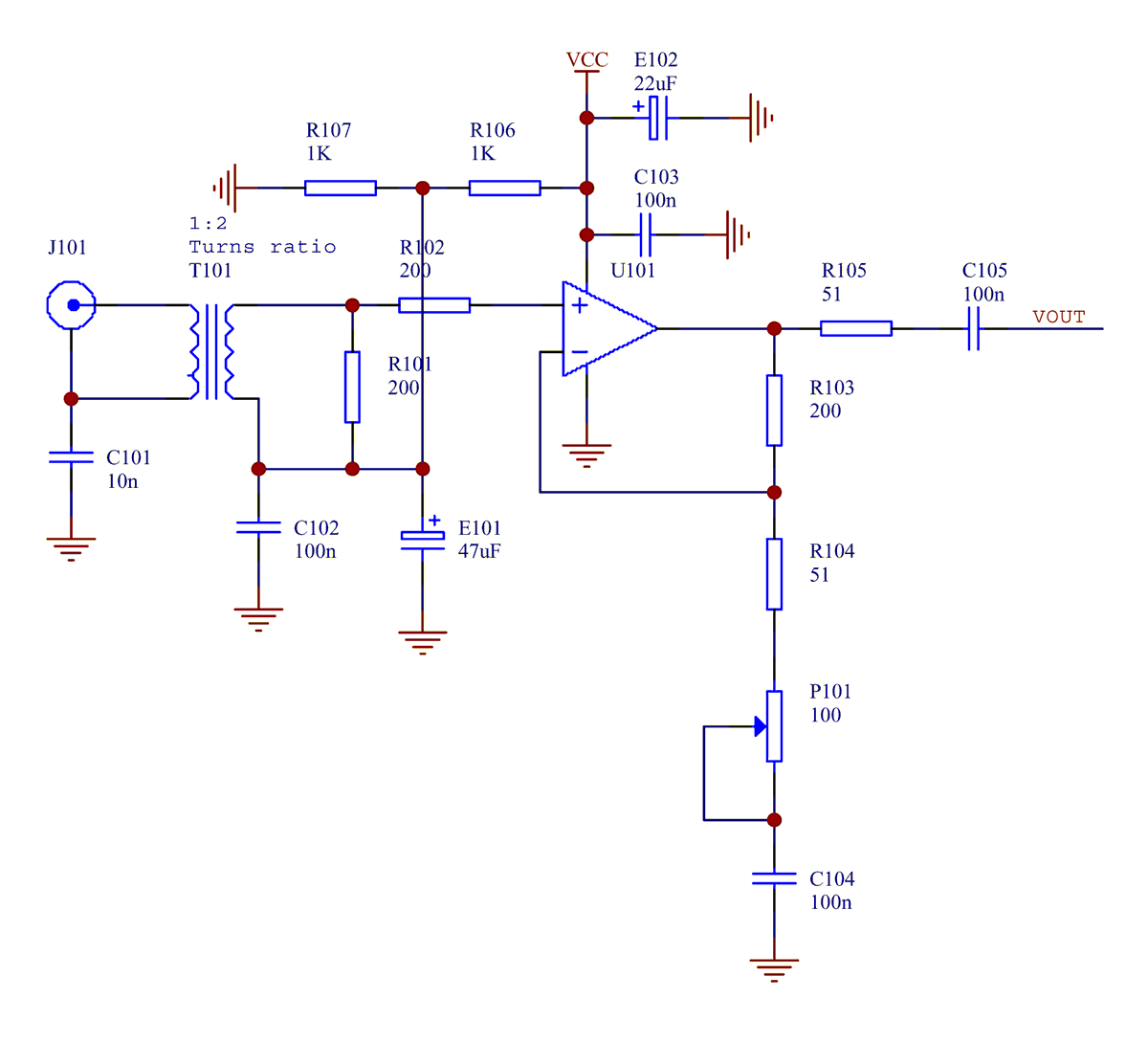
The circuit below illustrates a single supply variable gain RF amplifier using an opamp. The input transformer steps up the signal by 6dB to minimise the RF gain required. A noninverting amplifier is used as it has the lowest equivalent noise for low RF gains. C104 ensures that the opamp dc gain and low frequency gain is low minimising the low frequency noise voltages across internal junctions and hence the opamp self noise flicker phase modulation. The feedback network and input protection resistors values are low to keep their contribution to the noise floor well below that of the opamp. C104 also ensures that the dc current flowing in the feedback resistor network is very low so that a cermet pot can be used in the feedback network without adding significant excess noise. R101, R102, E101, C102 are used to generate a low noise voltage divider to bias the transformer secondary and opamp noninverting input at 1/2 the supply voltage.
 |
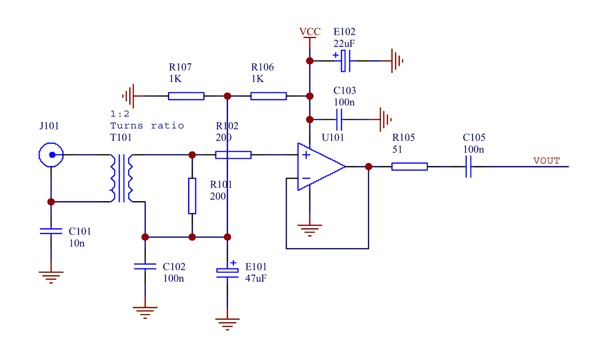
The circuit below illustrates a single supply unity gain RF amplifier using an opamp. The input transformer steps up the signal by 6dB to minimise the RF gain required. A noninverting amplifier is used as it has the lowest equivalent noise for low RF gains. The opamp noise gain is unity minimising the low frequency noise voltages across internal junctions and hence the opamp self noise flicker phase modulation. The feedback network and input protection resistors values are low to keep their contribution to the noise floor well below that of the opamp. R101, R102, E101, C102 are used to generate a low noise voltage divider to bias the transformer secondary and opamp noninverting input at 1/2 the supply voltage.
 |
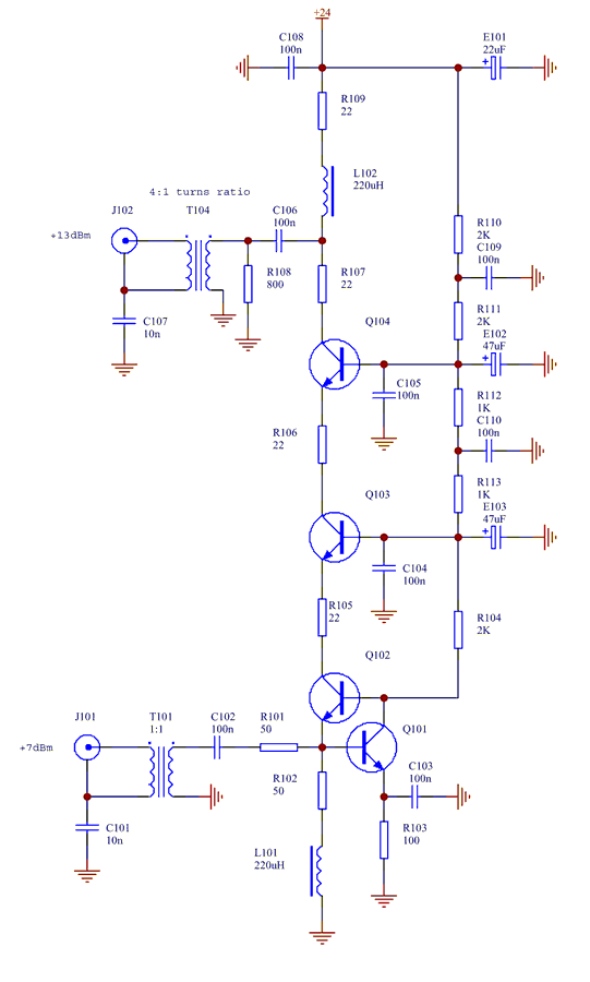
The lowest phase noise RF isolation amplifiers use discrete components rather than opamps. These RF isolation amplifiers can have a phase noise floor 10dB or more below that achievable using opamps. However it can be difficult to achieve low distortion unless power hungry differential amplifiers are used. Distortion can occur due to variation of current gain with current, modulation of the output capacitance of a stage by large signals. If the signal is converted to a current using a common base stage then by cascoding the input stage twice with additional common base stages the reverse isolation can be very high and the distortion of the emitter current of the output stage can be -60dBc or less. Unless the output stage collector load is kept low the output signal distortion may be as high as -40dBc unless a differential common base output stage is used.
In the circuit below Q101 reduces input distortion significantly by correcting for the nonlinearity of the emitter impedance of Q102. However the high impedance load at Q104 collector increases the output distortion. The noise floor can be typically reduced by 2dB to 3dB if Q102, Q103, Q104 are replaced by appropriately biased darlington pairs.
 |
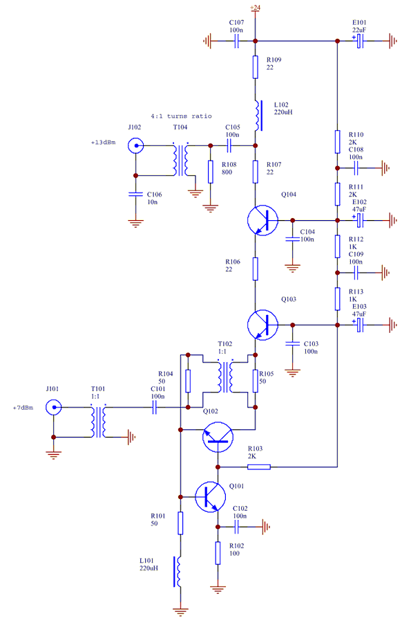
In the circuit below Q101 reduces input distortion significantly by correcting for the nonlinearity of the emitter impedance of Q102. However the high impedance load at Q104 collector increases the output distortion. The transformer feedback from the collector of Q102 is quieter than the equivalent resistive series at the emitter. The noise floor can be typically reduced by 2dB to 3dB if Q102, Q103, Q104 are replaced by appropriately biased darlington pairs.
 |
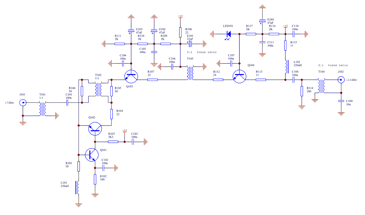
In the circuit below Q101 reduces distortion significantly by correcting for the nonlinearity of the emitter impedance of Q102. The low imedance at the collector of Q104 ensures that the output distortion is relatively low. Transformer feedback from the collector of Q102 is quieter than the equivalent series resistive feedback at the emitter. The noise floor can be typically reduced by 2dB to 3dB if Q102, Q103, Q104 are replaced by appropriately biased darlington pairs.
 |
TBC..
1) A New 5 and 10MHz High isolation Distribution Amplifier
2) Origin of 1/f PM and AM Noise in Bipolar Junction Transistor Amplifiers
3) Guidelines for designing BJT Amplifiers with Low 1/f PM and AM Noise
4) A Low Noise 100MHz Distribution Amplifier for Precision Metrology
5) PM Noise Generated by Noisy Components
6) A Practical Guide to Isolation Amplifier Selection