Often a low noise power supply is required to power a VCO an OCXO or an isolation amplifier. These are not usually off the shelf items so you may have to build your own. Here are some guidelines:
The output noise of a regulator (neglecting the effect of regulator input power supply noise) is determined by the reference noise, the error amplifier input noise and the error amplifier closed loop gain. Within the regulator bandwidth the output noise (Vn) of a conventional voltage regulator is given by:
Vn = G*(√(Enref2 + Enamp2 + In2Req2 + 4kTBReq))
where:
G is the closed loop gain
Enref is the reference noise at the input to the error amplifier
Enamp is the error amplifier equivalent input noise voltage
In is the error amplifier input current noise
Req is sum of the resistances seen by the error amplifier inputs
k is Boltzmann's Constant (1.38x10⁻²³ J/K)
T is the temperature in Kelvin
B is the Bandwidth in Hz.
The noise can be reduced by:
1) Reducing G (use a capacitor to bypass the resistor connected
between the error amplifier input and the regulator output - take
care to ensure this doesn't degrade the regulator phase margin)
2) Low pass filtering the reference seen by the error amplifier
3) Minimise Req to minimise resistor Johnson noise term and the the In*Req term
The venerable 723 is a good benchmark for comparing low noise regulators. For this regulator in the 100Hz to 10kHz band the regulator noise parameters are:
The reference noise is somewhat larger than the noise of a good buried zener reference (50-100nV/√Hz) in the 100Hz to 10kHz band and is even worse below 100Hz. This indicates that lower noise can be achieved (limited by the error amplifier noise) by substituting a low noise buried zener reference (e.g. LM329) for the internal reference.))
The error amplifier equivalent input noise voltage is also significantly larger than that of a modern low noise opamp. Thus a discrete regulator using a low noise buried zener reference and a low noise opamp as the error amplifier combined with a discrete series pass transistor and driver can have a much lower output noise than the equivalent 723 regulator.
In practice filtering out the reference low frequency (<100Hz)noise components can be difficult to achieve. In this spectral region the noise can be reduced by:
1) An active low pass filter (darlington emitter follower
buffered RC filter). A filter time constant of a few seconds is
readily achieved however the emitter follower will degrade the
output voltage tempco over that of the voltage regulator circuit and
reduce the supply voltage by at least a couple of Vbe drops.
2) By using the average output of several low noise buried zener
references. Directly connecting several buried zeners in parallel as
advocated by some is unlikely to be useful as the zener voltages
must track within impractical tolerances to equalise the current
flowing thorough an consequently the noise of each zener.
3) Where possible increase the current in the buried zener (its not
possible to change the current flowing in the internal buried zener
within an LM329).
As suggested by Said Jackson the power supply output may be low pass filtered by a low value resistor (2 ohms??) and a high value electrolytic capacitor (10,000 μF) Actual component values depend on the load characteristics.
1) Be skeptical of manufacturers claims. Work out the regulator
output noise for the voltage output you require.
2) Choose a regulator where the internal reference noise can be low
pass filtered.
Measuring Power supply noise is complicated by the fact that there is a large dc offset at the power supply output. Using an AC coupled preamp to amplify the noise to a suitable level for measurement by a spectrum analyser requires using large coupling capacitors for measurement at low frequencies. Increasing the input resistance of the preamp to allow use of smaller coupling capacitors isn't a useful option as it increases the amplifier input noise. Input coupling capacitor charging transients can easily destroy a preamp input stage unless suitable protection circuitry is used. However such protection circuitry add noise. Schemes such as precharging the coupling capacitor before connecting it to the preamp input add complexity and can be ineffective if careful sequencing of the precharge sequence isn't adhered to.
|
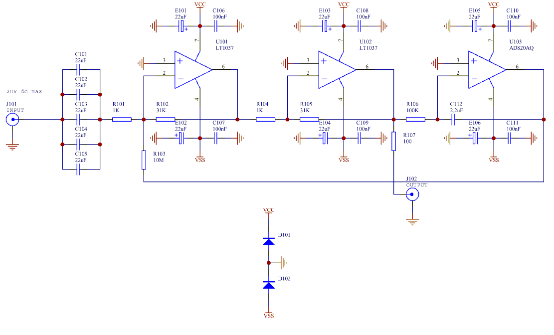
In the above preamp R101 limits the input coupling capacitor charging transient current flowing in the input amplifier input protection diodes. The thermal noise of R101 also adds to the preamp input noise. The maximum current ratings of U101's input protection diodes limit the maximum dc voltage of the power supply under test to about 20V.
TBC...
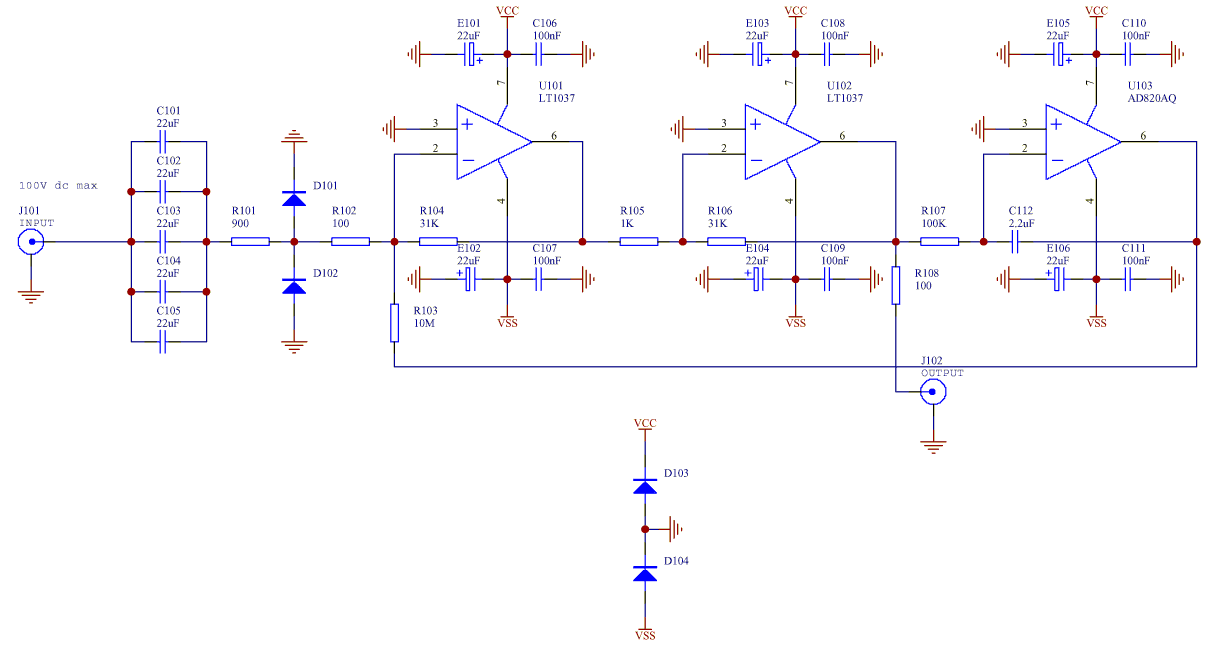 |
In the above preamp R101 limits the input coupling capacitor charging transient current flowing in the shunt diodes D101 and D102. R102 limits the current flowing through U101's input protection diodes. With suitable choice of D101 and D102 a much higher output voltage power supply can be tested than with the previous circuit.
TBC...
The system noise floor can be reduced below the input noise of the preamp by using correlation techniques.
2 amplifiers are connected to the power supply output and by averaging several cross power spectra of their outputs the system noise can be reduced by 20dB or more depending on the cross talk between spectrum analyser channels and the number of cross power spectra averaged..
TBC...
It is possible to extend the low frequency cutoff if a stack of low noise batteries is used to oppose the power supply output and an autozero circuit is used to remove the residual dc (1/2 battery cell voltage max). However great care (or provision of suitable input protection circuitry ) is needed with connection and supply power-up/power-down sequencing to avoid destroying the preamp input stage.
TBC...
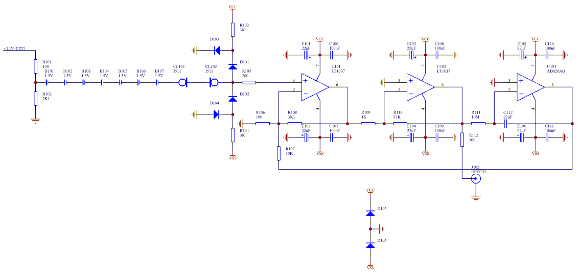 |
In the above circuit which is setup to amplify the low frequency noise of an 11V power supply a series stack of 7x1.5V batteries produces a low noise 10.5V supply which reduces the dc voltage seen by the amplifier to near zero. R101 and R102 are selected to produce a voltage at the divider tap equal to the voltage of the battery stack. The dc servo compensates for up to 100mV of residual dc input. The preamplifier low frequency cutoff is about 7.2 millihertz. The use of batteries to offset the power supply dc output was suggested by Poul-Henning Kamp. The resistive divider and the servoloop extend the method to power supply voltages not equal to an integer multiple of the battery voltage and compensate for battery voltage thermal drift.
Current limiter diodes CL101 and CL102 limit the current flowing in the clamp diodes when the input voltage is large (e.g. when the batteries are not present or the supply under test is shorted out). Maximum dc input is 50V dc.
TBC...