|
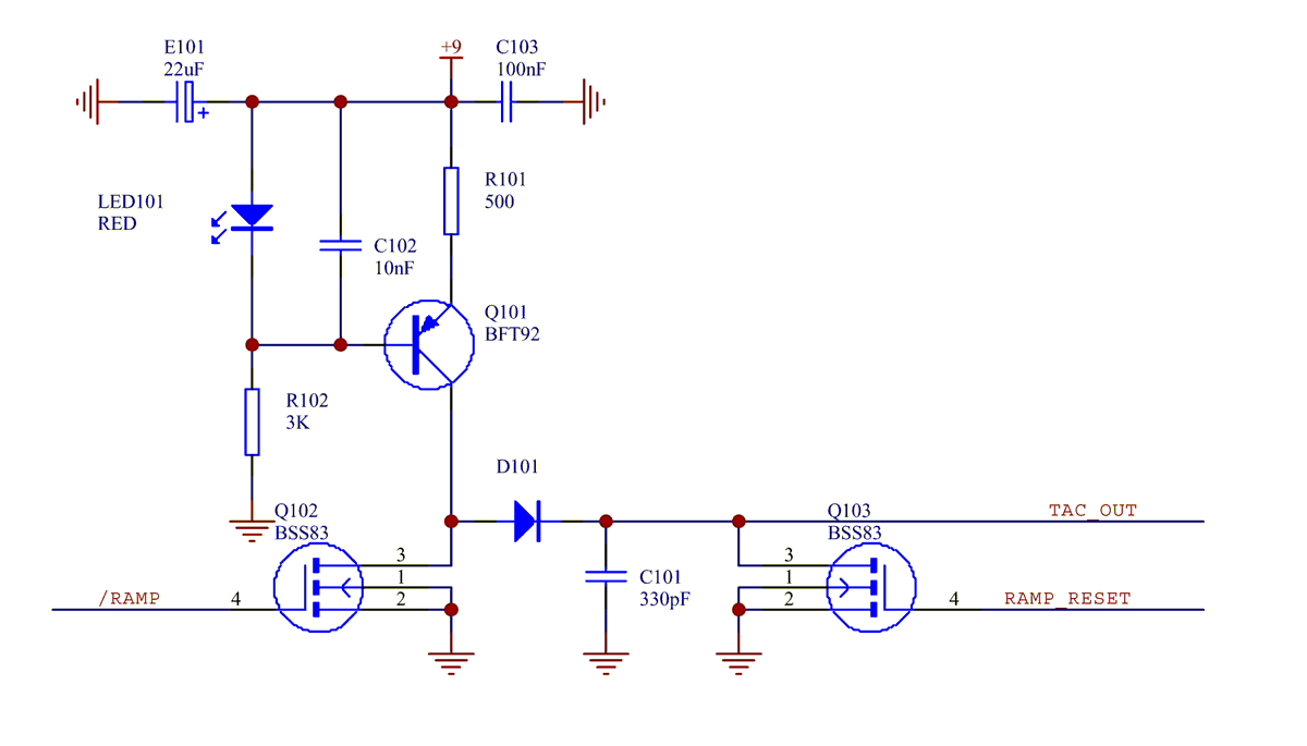
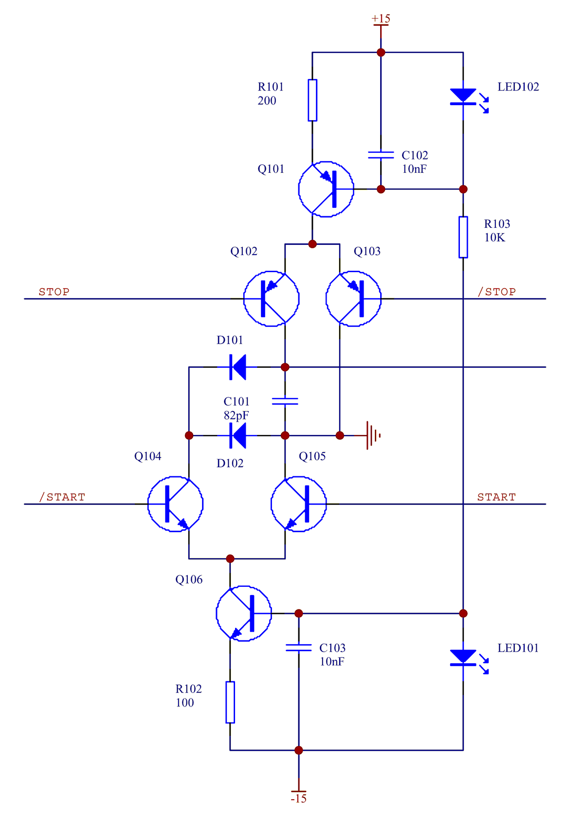
In the above circuit ramp capacitor discharge switch gain Q103 and ramp switch transistor Q102 are both on ensuring that the ramp capacitor (C101) voltage is near zero. To measure the width of a short pulse, The ramp reset switch Q103 is first turned off by the leading edge of the pulse and then after a short fixed delay Q102 is turned off for a period equal to the pulse width to be measured. When Q102 is turned back on the voltage across the ramp capacitor is proportional to the duration of the pulse being measured. In effect Q101-Q103 etc comprise a time to amplitude converter or TAC. The ungrounded ramp capacitor node is typically connected to the input of a charge redistribution ADC with a high (capacitive) input impedance. At the completion of the ramp charging phase this ADC converts the ramp voltage to produce a digital output. The circuit has a range of 400ns and a 0-2.5V ramp output voltage range.
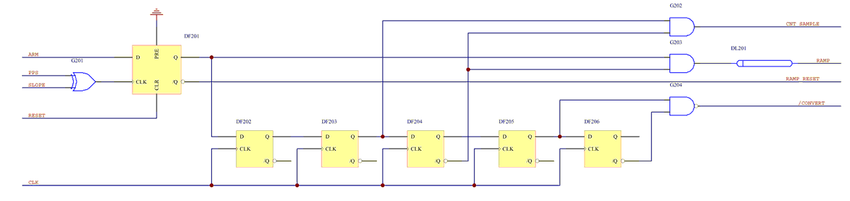 |
Typically as depicted in the circuit above, such a TAC may be used to measure the input to output delay of a synchroniser circuit used to synchronise a pulse edge to a clock. The synchroniser output samples a continuously clocked counter. Combining the sampled count with the TAC ADC output allows interpolation between clock edges to produce a high resolution time stamp.
1) The finite current flowing through D101 when Q102 and Q103 are on produces a voltage drop across Q103's on resistance.
2) Charge injection when Q103 switches off.
3) Charge injection when Q102 switches off and on.
1) The finite output resistance of the current source transistor Q101.
2) The voltage dependence of the current source transistor output capacitance.
3) The voltage dependence of the ramp reset transistor capacitance.
4) The voltage dependence of the switching diode (D101) capacitance.
5) The voltage dependence of the ADC input capacitance
6) the voltage dependence of the switching diode reverse current.
1) The charge current source tempco.
2) The ramp capacitor tempco.
3) The current source output capacitance and resistance tempcos.
4) The diode capacitance tempco.
5) The output capacitance tempco of Q103.
6) The ADC input capacitance tempco.
1) The effect of TAC tempco and nonlinearities can be corrected by calibration. In particular calibration pulse with widths of say 1,2,3,4 clock cycles can be interleaved between input signal measurements. This is easy to do when the signal being time stamped has a low repetition rate as when timestamping the leading edge of a PPS pulse from a GPS timing receiver or generated from a clock source by a frequency divider.
2) Such calibration techniques do not allow the TAC offset to be measured to an accuracy of better than a gate propagation delay. Usually more than one channel is used with one TAC interpolator per channel. In analysing the time stamp sequences only the offset differences between channels and not the absolute offset of a particular channel is important. The relative offset of all channels are easily determined by driving all channels simultaneously with the same calibration signal.
3) Q102 and Q103 can be replaced by 2 open drain inverters from a 74AC05, however the output capacitance is higher and output switch leakage current is not tightly controlled. Do not use the other 4 inverters in the 74AC05 as doing so is likely to increase the propagation delay jitter.
4) If a gate array is used to implement the synchronisers the circuit timing noise will increase to a few tens of picoseconds. If dedicated SSI logic is used to implement the critical portions of the control logic (synchroniser, calibration pulse retiming) then timing noise can be as low as a few picosec. Non critical functions such as ADC control, ramp reset, etc can be implemented in a gate array without significant impact on the system noise.
5) The propagation delay of the delay element isn't too critical. The delay has to be long enough to ensure the ramp reset switch is turned off before the ramp capacitor begins to charge. The propagation delay of the delay element has to have good short term (between autocalibration cycles) stability and low jitter.
6) The resolution can be increased by using a 14 or 16 bit DAC and by decreasing the TAC input range. A higher frequency clock is then required for the synchroniser and control logic. A resolution of a few picosec can be achieved, however linearity correction and frequent autocalibration is required.
7) When the TAC circuit is integrated into a custom IC using a high frequency BICMOS process a resolution of 1ps (with subpicosecond noise) can be achieved.
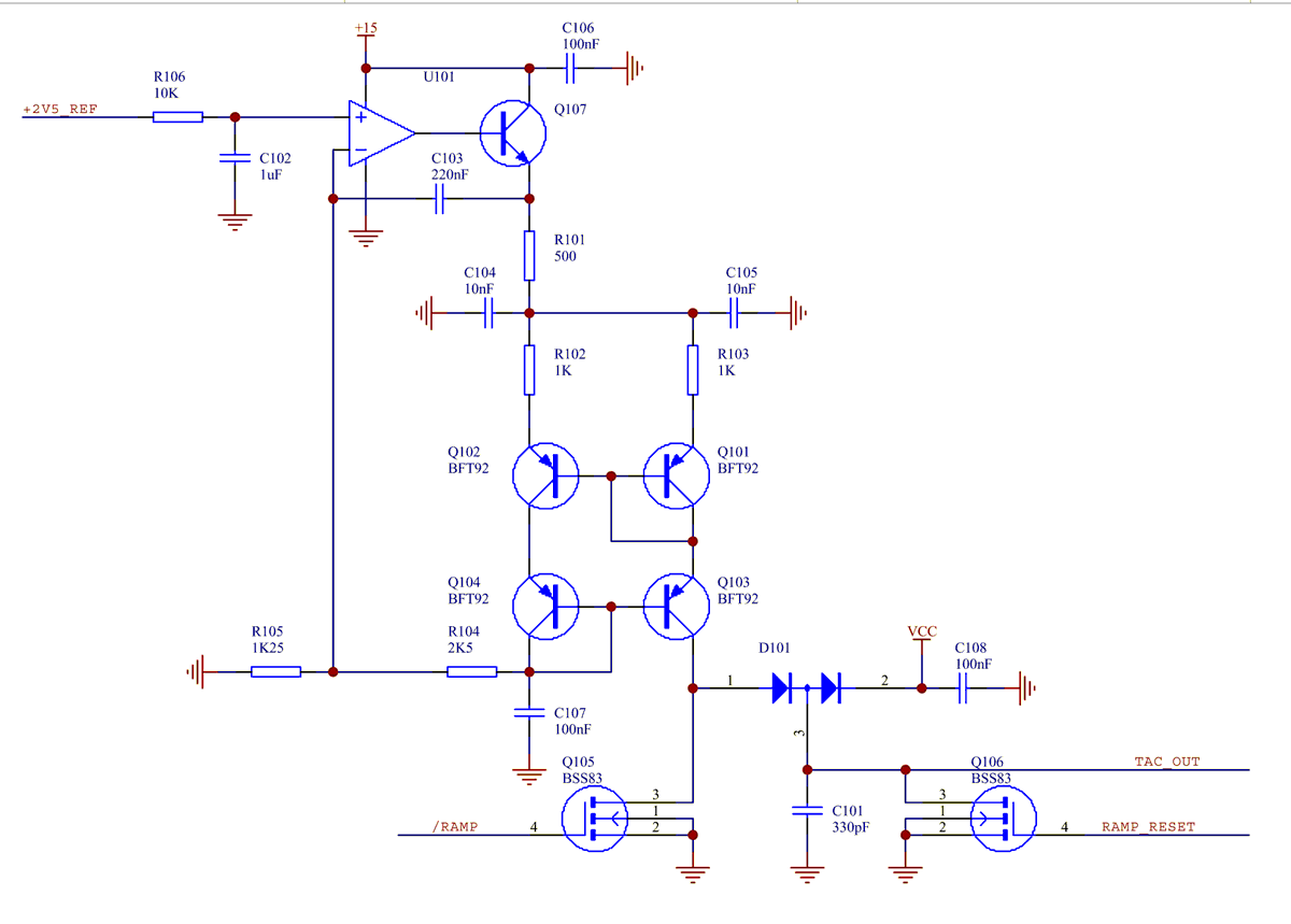 |
In the circuit above the current source is a high output resistance Wilson current mirror (Q101-Q104). Opamp U101 sets the current mirror current flowing into the mirror as VREF/R104. If the 2.5 volt reference tracks the ADC reference then the ADC reference tempco doesn't affect the TAC gain which then only depends on capacitor ratios, resistor ratios, transistor matching and an RC product. The dual diode provides some compensation for diode leakage and capacitance variations over the part of the TAC range that is actually used.
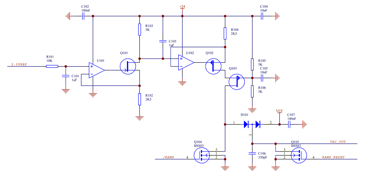 |
In the circuit above the current source is a high output resistance cascoded PJFET current source. Opamp U101 and U102 ensure that the ramp charging current tracks the ADC reference voltage. Low pass filtering the reference and using PJFETs with low gate current reduces the ramp charging current noise to about 1/2 that of the simple single BJT current source circuit. This ensures that the ADC noise dominates the TDC noise.
 |
When designing a TAC to measure short time intervals it is desirable to increase the TAC capacitor charging current so that a relatively large ramp capacitor can be used to minimise the effect of stray capacitances, This is particularly important when using a discrete implementation. However increasing the capacitor charging current increases the voltage drop across the FET switch used in the preceding circuits.
The above circuit overcomes the problem of the voltage drop in the reset switch by using a pair of matched diodes as the reset switch. During reset the diode currents and forward drops are nominally equal so that the voltage across the ramp capacitor is small. To ensure equal diode currents during reset the tail current of the START long tailed pair must be twice that of the STOP long tailed pair.
The circuit doesn't show the level translators required to translate from the logic levels to the long tailed pair inputs. The START pulse width must be sufficient to ensure the TAC voltage is sampled by the ADC before the circuit is reset. A START and STOP flipflops can be used to ensure the STOP and START pulse widths are adequate. For low duty cycle signals such as a PPS signal from a GPS timing receiver AC coupling with dc restoration can be used to accomplish the required level shifting for the START and STOP long tailed pair current switches.
TBC...