|
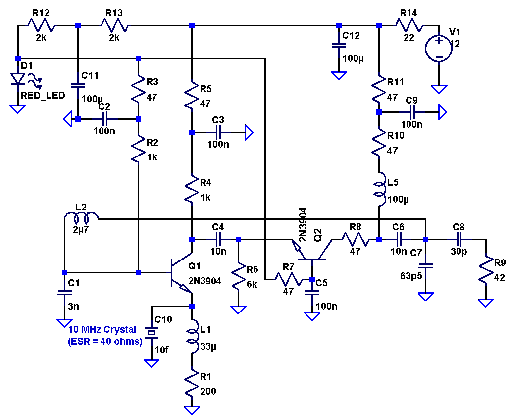
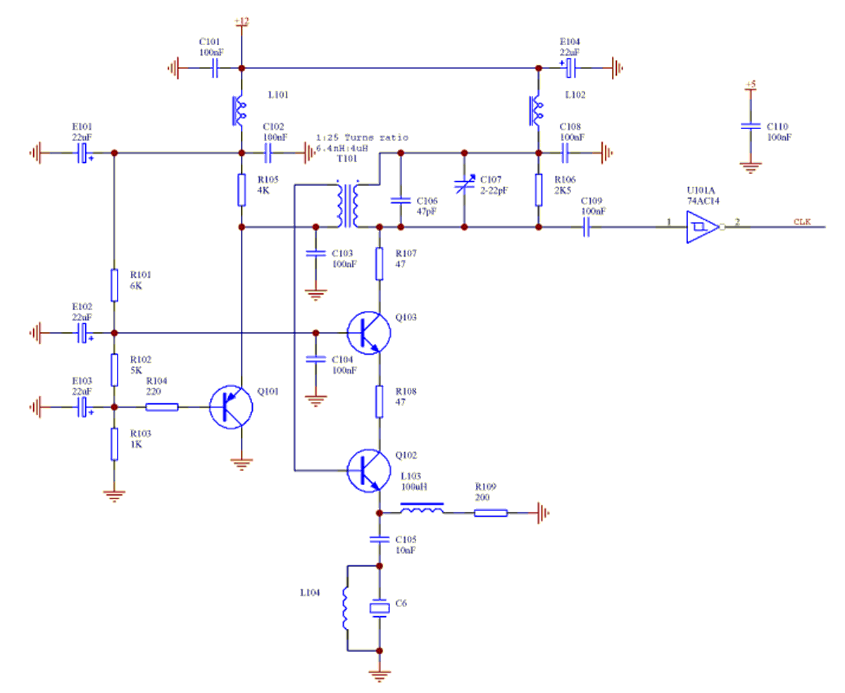
The oscillator comprises Q1 and Q2. Q1 operates in class A and its collector is coupled to the emitter of common base stage Q2 whose collector tank circuit drives the base of Q1. Common base stage Q2 buffers the oscillator from the load. The emitter current of Q2 is less than that of Q1 so that Q1 is driven into cutoff limiting the crystal current. Replacing R4 by an inductor is a bad idea as Q2's base emitter junction will enter zener breakdown during part of the cycle. Q2 also saturates during part of the cycle and the crystal current is poorly controlled. However shunting R4 with a 100uH inductor to reduce the dc gain from base to collector of Q1 may be useful in that it reduces the flicker phase phase noise of Q1.
LED D1 ensures that the emitter currents of Q1, and Q2 have a low tempco.
Other versions use a tapped inductor, instead of a capacitive divider, in the tank to provide feedback to the base of Q1.
TBC...
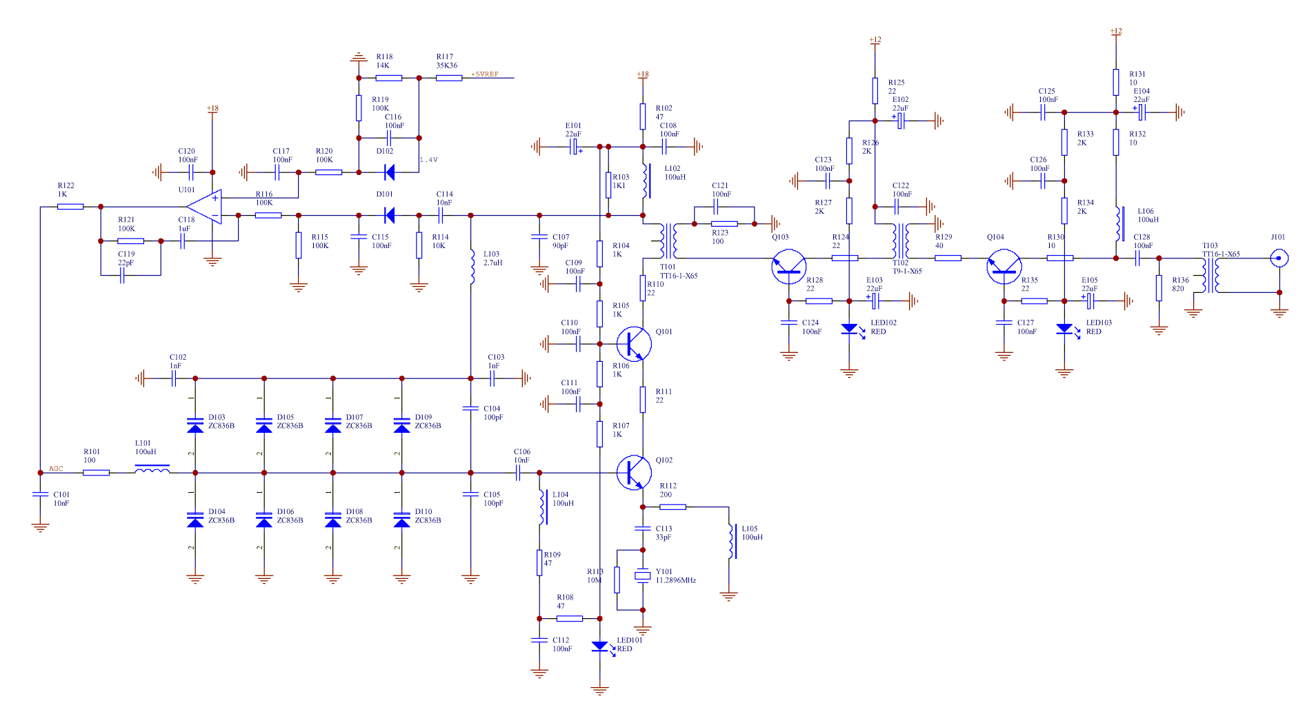 |
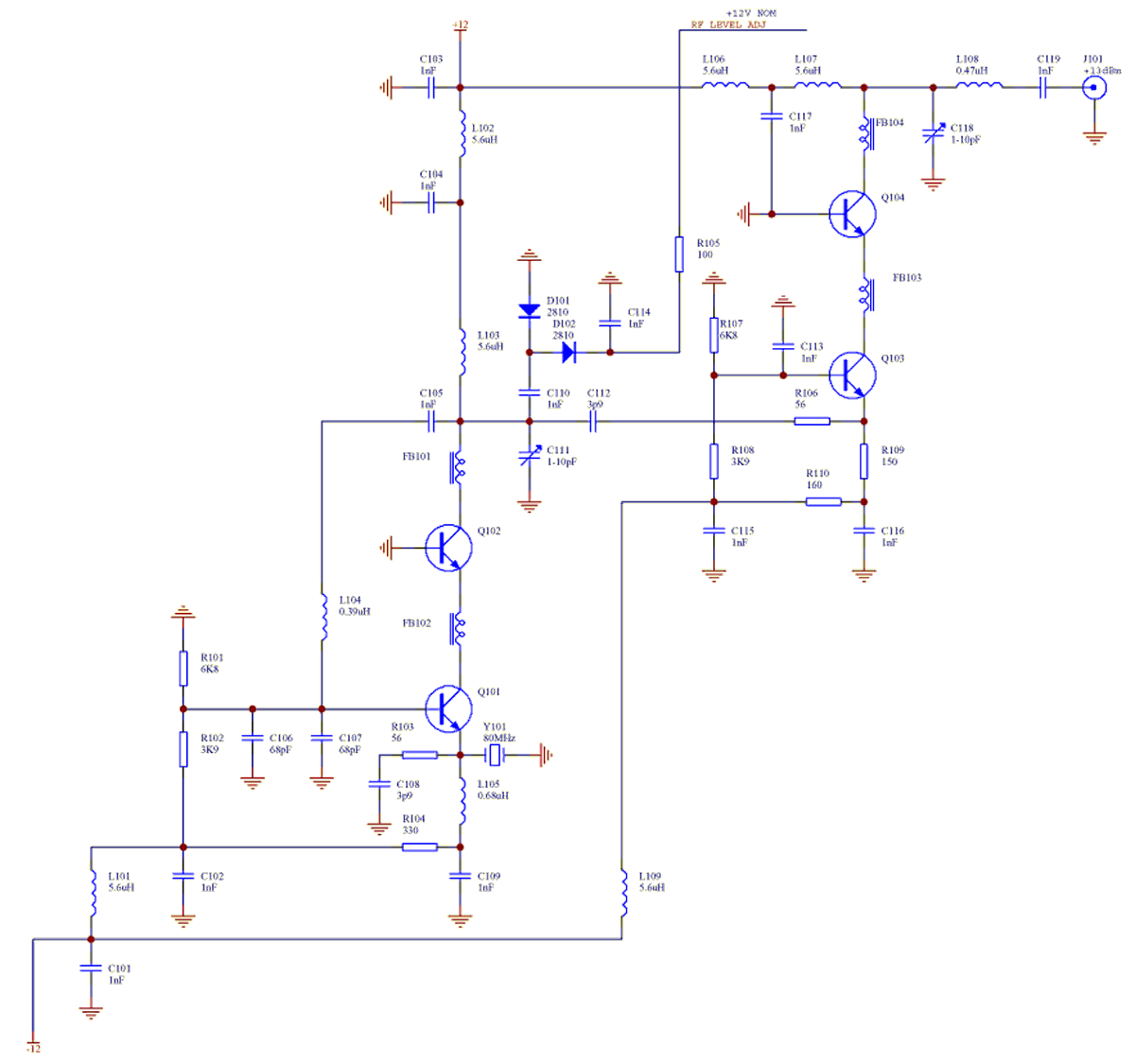
This oscillator uses a variable capacitive attenuator to provide AGC. The appropriate AGC circuit time constant depends on the crystal bandwidth. Diodes D101 peak detects the RF voltage at the collector of Q102. D102 and its associated resistors compensate for the forward drop of D101 and set the peak Rf voltage at Q102 collector to 1.4V. T101 couples the RF collector current of Q102 to the buffer amplifier (a pair of cascaded transformer coupled common base stages). The low impedance at Q101 base together with the relatively high emitter current of Q101 ensure that the real part of the emitter impedance seen by the crystal is low so that the crystal operating Q is high. For fundamental crystals a higher crystal current is desirable and the values of the collector tank (L, C and R) components should be adjusted accordingly.
Since the entire oscillator operates in class A it should have somehat lower noise than the preceding oscillators in the flicker noise region.
Correct phasing of the windings of T101 and T102 reduces the dc magnetisation of the cores. Since no compensating current source is available for the secondary of T103 a capacitor coupled shunt feed scheme is used to avoid having the collector current of Q104 saturate the transformer core.
LED101, LED102, LED103, LED104 ensure that the emitter current of Q101, Q102, Q103 and Q104 respectively, has a low tempco.
TBC...
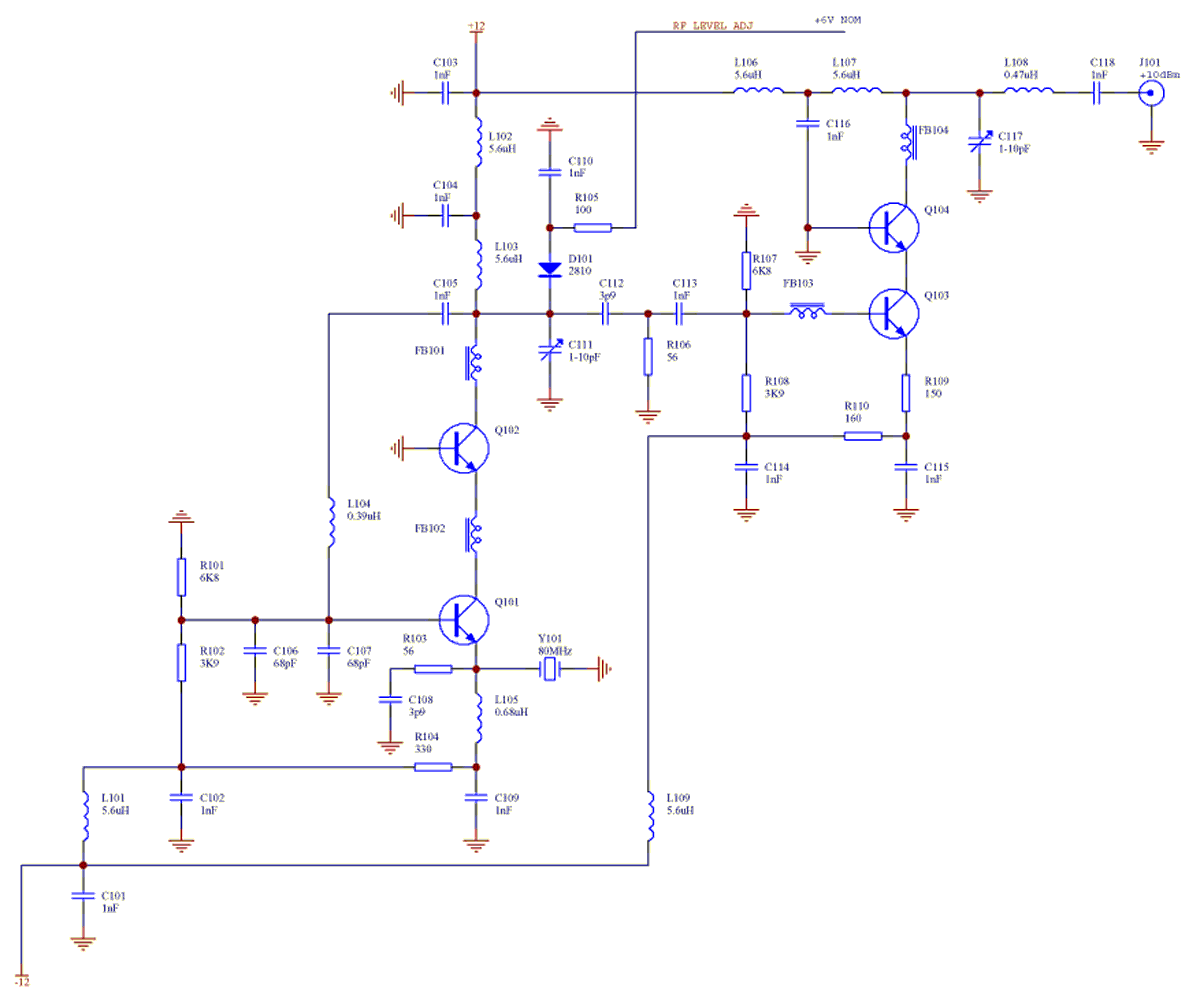 |
The above oscillator uses an 80MHz 5th overtone high inductance crystal.
Diode D101 limits the swing at the collector of Q102. Q103 and Q104 are configured as a cascode buffer.
Q101-Q104 should have an ft of 1GHz or more. Original transistors were 2N2857
TBC...
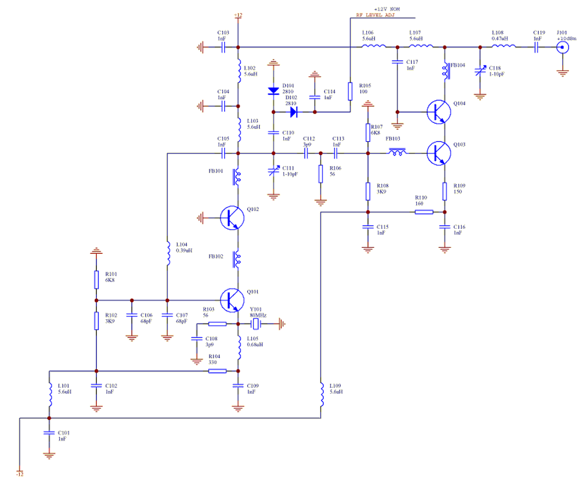 |
Above version has improved limiting circuit.
TBC...
 |
This version has higher output, better load isolation and lower noise floor.
TBC...
 |
The above oscillator has low phase noise and relatively few parts. However winding the transformer will be difficult and a capacitively tapped tank circuit may actually be easier to build.
TBC...