(More Info) |
Bruce's: Zero Crossing Detectors
A seminal paper on optimal zero crossing detector design was published by Oliver Collins in 1996 ("The Design of Low Jitter Hard Limiters" IEEE transactions on Communications, Vol 44 No 5, May 1996 pp 601-608)* Collins shows how to account for the effect of clamping diodes on the output noise of a limiter/filter stage. He shows that the optimum limiter consists of a relatively large number of cascaded limiter/filter stages with the gain of and bandwidth of each successive stage larger than its predecessors. In practice a ZCD consisting of as few as 6 cascaded stages or even less may have a performance not significantly worse than the theoretical optimum.
This paper is available for purchase (you dont have to be an IEEE member) on line from the IEEE, or if you are lucky may be found at a library that subscribes to this particular IEEE journal.
The file (Generalised Collins Hard Limiter ) extends the Collins analysis to include the common case where the the equivalent input noise of each limiter/filter stage are all different.
The following set of guidelines are useful for calculating the equivalent input noise for non inverting and inverting filter/limiter stages.
Non inverting limiter/filter stages
In the above circuit the dc gain is (1 + R102/R101).
When calculating the jitter contribution of this stage the effective input noise includes:
- The amplifier input noise voltage
- The noise voltage produced by the amplifier input noise current flowing through R101||R102
- The noise voltage produced by the input noise current of the next stage flowing through R103 divided by the dc gain.
- The Johnson noise of R101||R102
- The Johnson noise of R103 divided by the dc gain
NOTES
For the first stage the mixer output noise contributes to the effective input noise of the first stage.
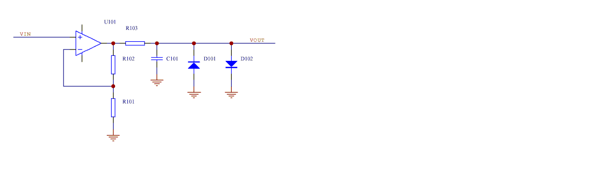
High gain stages
Sometimes the gain of the stage is too high to avoid amplifier saturation when using the above noninverting amplifier configuration. In this case additional clamp diodes across a portion of the feedback resistor may be required to avoid amplifier saturation as shown below.
In the above circuit the dc gain is (1 + (R103 +R102/R101) ) and the gain when either of the auxiliary diodes (D101, D102) is conducting (1+ R102/R101) is chosen to be larger than the minimum stable gain of U101. This can allow a decompensated opamp (e.g.. OP37) with a higher gain bandwidth but which isn't unity gain stable to be used.
TBC...
Inverting limiter/filter stages
In the above circuit the dc gain is -(R102/R101)
When calculating the jitter contribution of this stage the effective input noise includes:
- The opamp input noise voltage
- The noise voltage produced by the opamp input noise current flowing through R101||R102
- The Johnson noise of R101||R102
- The opamp input noise voltage of any preceding such inverting amplifier limiter stage
NOTES
- The opamp input noise voltage of this inverting stage contributes to the effective input noise of the following stage.
- For the first stage the mixer output noise contributes to the effective input noise of the first stage.
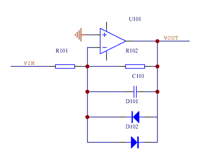
Alternative Inverting limiter/filter stages

In the above circuit the dc gain is -(R102/R101)
This circuit is useful for low gain low bandwidth stages. In particular when used as the ZCD input stage following the mixer it can be designed to limit the current injected into the mixer should the opamp output saturate near one of the supply rails as may occur when one of the opamp supply rails go to zero (or be disconnected). Diodes D101 and D102 (which may be internal to the opamp) clamp the inverting opamp node to ground in the event that the opamp output saturates, thus limiting the current flowing into the mixer via R101. At low mixer output beat frequencies the mixer output noise will be relatively large and it is easy to ensure that the amplifier's equivalent input noise contribution to the ZCD timing jitter is insignificant compared to the mixer output noise contribution to the ZCD timing jitter.
The low pass filter time components may be selected independently of the gain setting components. This is particularly convenient when only a limited range of low tempco capacitor values is available. The following amplifier/limiter stage should be a non inverting stage to avoid significantly loading the filter output.
When calculating the jitter contribution of this stage the effective input noise includes:
- The opamp input noise voltage
- The noise voltage produced by the opamp input noise current flowing through R101||R102
- The Johnson noise of R101||R102
- The Johnson noise of R103 divided by the stage dc gain.
- The opamp input noise voltage of any preceding inverting amplifier-limiter stage with the filter cap connected across the feedback resistor
NOTES
- The opamp input noise voltage of this inverting stage does not contribute to the effective input noise of the following stage.
- For the first stage the mixer output noise contributes to the effective input noise of the first stage.
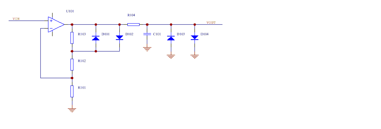
High gain wide bandwidth stages
Sometimes,particularly for the last high gain wide bandwidth stage of the filter limiter cascade, it is difficult to achieve the required gain and bandwidth using a single opamp, especially if the phase shift contribution of the opamp is to be kept small so that the phase shift and delay is dominated by the passive filter components. In this case a wideband opamp like an AD829 with external compensation can be useful. Sometimes even the AD829 has inadequate gain bandwidth so that a cascaded pair of opamps as illustrated below may be required. A current feedback opamp like an AD811 can often be used as the second opamp without major effect on the effective input flicker noise of this stage.
TBC...
ZCD Phase shift tempco
The phase shift tempco of a ZCD is dominated by the tempco of the low pass filter components used in the fist stage output low pass filter. A high performance 5 stage Collins style ZCD design with a 10Hz input beat frequency may have a first stage output RC filter time constant of around 2 millisec. Even when a resistor with a tempco of 15ppm/C or less are used together with NPO/C0G capacitor the phase shift tempco for a 10MHz mixer input frequency may be as high as 10-20fs/C. Subsequent stages have equivalent output filter phase shift tempcos less than 1/2 this. Consequently the temperature of the pair of ZCD's used in a DMTD system should track to better than 1C to avoid degrading the system performance.
When mixer output noise dominates ZCD noise
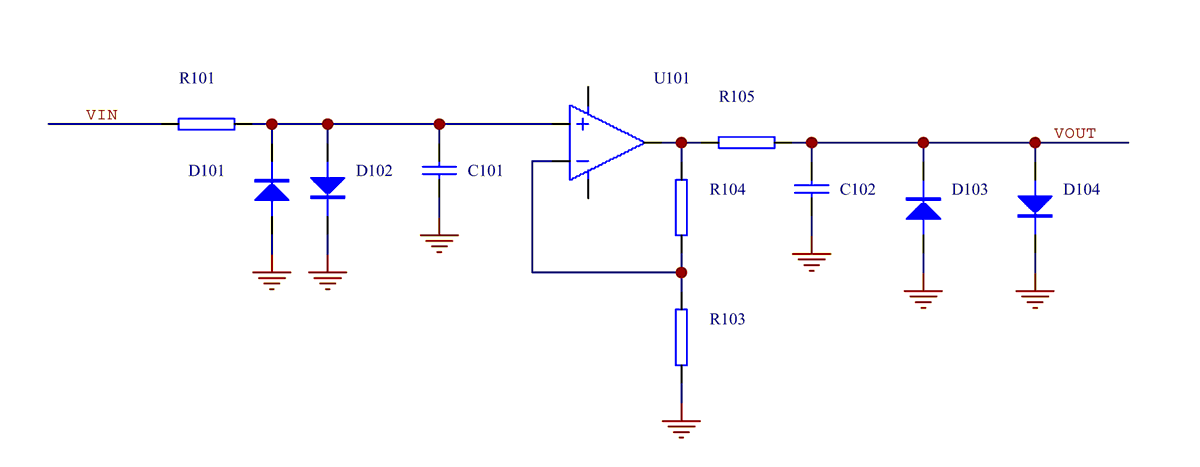
Often, particularly with low mixer output beat frequencies, the mixer output noise is much greater than input noise of the ZCD gain stages. In this case the optimum input stage dc gain is close to 1 and this stage can be replaced with a passive RC filter with a diode clampled output without significantly increasing the ZCD output jitter. Such a filter also has the beneficial effect of protecting the mixer from the consequences of disconnecting one of the following amplifier's power supplies.
As illustrated in the circuit diagram below it is convenient to use a noninverting amplifier for the stage following the input RC filter.
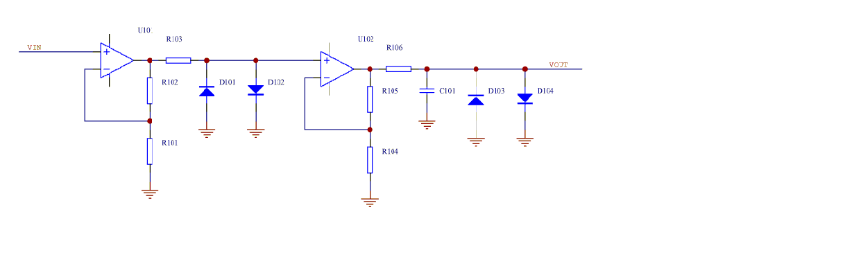
ZCD Design Example
Given a mixer with a 10Hz 0.7V pp trapezoidal beat frequency output with a zero crossing slew rate of 50V/s. A ZCD slope gain of 100,000 is required to achieve a 5V/μs ZCD output slew rate.
If the input noise is 10nV/√Hz for all ZCD stages and a 6 stage ZCD is used then the optimum filter time constants and dc gains for each stage are:
| Mixer output amplitude (V pk) |
Mixer output zero crossing slew rate (V/s) |
Mixer output frequency (Hz) |
| 0.35 | 50 | 10 |
| Stage | Input Noise (nV/√Hz) | Gain | Filter Time Constant |
| 1 | 10 | 2.83 | 5.33ms |
| 2 | 10 | 3.18 | 1.68ms |
| 3 | 10 | 4.01 | 418μs |
| 4 | 10 | 6.4 | 65.3μs |
| 5 | 10 | 16.29 | 4.01μs |
| 6 | 10 | 105.44 | 38ns |
The resultant zero cossing detector output jitter is about 2.4ns rms.
Design Tools
Spreadsheet for calculating stage gain and low pass filter time constant: Hard limiter design (Excel format)
Hard Limiter Design (Open Office format)
The spreadsheets were created by Roberto A (Italy).
TBC...